Cutting edge transistors for semiconductors of the future
Transistors that can change properties are important elements in the development of tomorrow’s semiconductors. With standard transistors approaching the limit for how small they can be, having more functions on the same number of units becomes increasingly important in enabling the development of small, energy-efficient circuits for improved memory and more powerful computers. Researchers at Lund University in Sweden have shown how to create new configurable transistors and exert control on a new, more precise level.
– Published 11 August 2023
In view of the constantly increasing need for better, more powerful and efficient circuits, there is a great interest in reconfigurable transistors. The advantage of these is that, in contrast to standard semiconductors, it is possible to change the transistor’s properties after they have been manufactured.
Historically, computers’ computational power and efficiency have been improved by scaling down the silicon transistor’s size (also known as Moore’s Law). But now a stage has been reached where the costs for continuing development along those lines have become much higher, and quantum mechanics problems have arisen that have slowed development.
Alternative to silicon
Instead, the search is on for new materials, components, and circuits. Lund University is among the world leaders in III-V materials, which are an alternative to silicon. These are materials with considerable potential in the development of high-frequency technology (such as parts for future 6G and 7G networks), optical applications, and increasingly energy-efficient electronic components.
Ferroelectric materials are used in order to realize this potential. These are special materials that can change their inner polarisation when exposed to an electric field. It can be compared to an ordinary magnet, but instead of a magnetic north and south pole, electric poles are formed with a positive and a negative charge on each side of the material. By changing the polarisation, it is possible to control the transistor. Another advantage is that the material “remembers” its polarization, even if the current is turned off.
An extremely small scalee
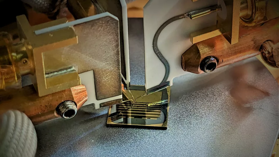
Through a new combination of materials, the researchers have created ferroelectric “grains” that control a tunnel junction – an electrical bridging effect – in the transistor. This is on an extremely small scale – a grain is 10 nanometres in size. By measuring fluctuations in the voltage or current, it has been possible to identify when polarisation changes in the individual grains and thus understand how this affects the transistor’s behavior.
The newly published research has examined new ferroelectric memory in the form of transistors with tunnel barriers in order to create new circuit architectures.
“The aim is to create neuromorphic circuits, i.e. circuits that are adapted for artificial intelligence in that their structure is similar to the human brain with its synapses and neurons,” says Anton Persson, who recently completed his doctoral degree in nanoelectronics.
What is special about the new results is that it has been possible to create tunnel junctions using ferroelectric grains that are located directly adjacent to the junction. These nanograins can then be controlled on an individual level, when previously it was only possible to keep track of entire groups of grains, known as ensembles. In this way, it is possible to identify and control separate parts of the material.
“In order to create advanced applications, you must first understand the dynamics in individual grains down to the atomic level, as well as the defects that exist. The increased understanding of the material can be used to optimize the functions. By controlling these ferroelectric grains, you can then create new semiconductors in which you can alter properties. By changing the voltage, you can thus produce different functions in one and the same component,” says Lars-Erik Wernersson, professor of nanoelectronics.
New memory cells
The researchers have also examined how this knowledge can be used to create different reconfigurable applications by manipulating in various ways the signal that goes through the transistor. It could, for example, be used for new memory cells or more energy-efficient transistors.
This new type of transistor is called ferro-TFET and can be used in both digital and analogue circuits.
“What’s interesting is that it’s possible to modulate the input signal in various ways, for example by the transistor shifting phase, frequency doubling, and signal mixing. As the transistor remembers its properties, even when the current is turned off, there is no need to reset it every time the circuit is used,” says Zhongyunshen Zhu, doctoral student in nanoelectronics.
Another advantage of these transistors is that they can function at low voltage. This makes them energy-efficient, which will be required, for example, in tomorrow’s wireless communication, Internet of Things, and quantum computers.
“I consider this to be leading-edge research of international standing. It’s good that in Lund and Sweden, we are at the forefront regarding semiconductors, especially in view of the EU’s recently enacted Chips Act, which aims to strengthen Europe’s position regarding semiconductors,” says Lars-Erik Wernersson.
Publication:
Link to the articles in Nature Communications and Science Advances:
Reconfigurable signal modulation in a ferroelectric tunnel field-effect transistor
Sensing single domains and individual defects in scaled ferroelectrics