LTH Profile Area: Nanoscience and Semiconductor Technology
Infrastructure
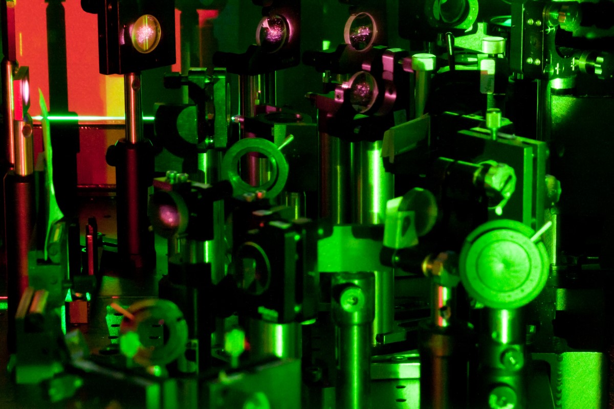
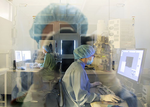
The infrastructures within the Profile Area involves Nano laboratories. The Profile Area is also engaged in MAX IV. Links below will open the respective infrastructure's website.
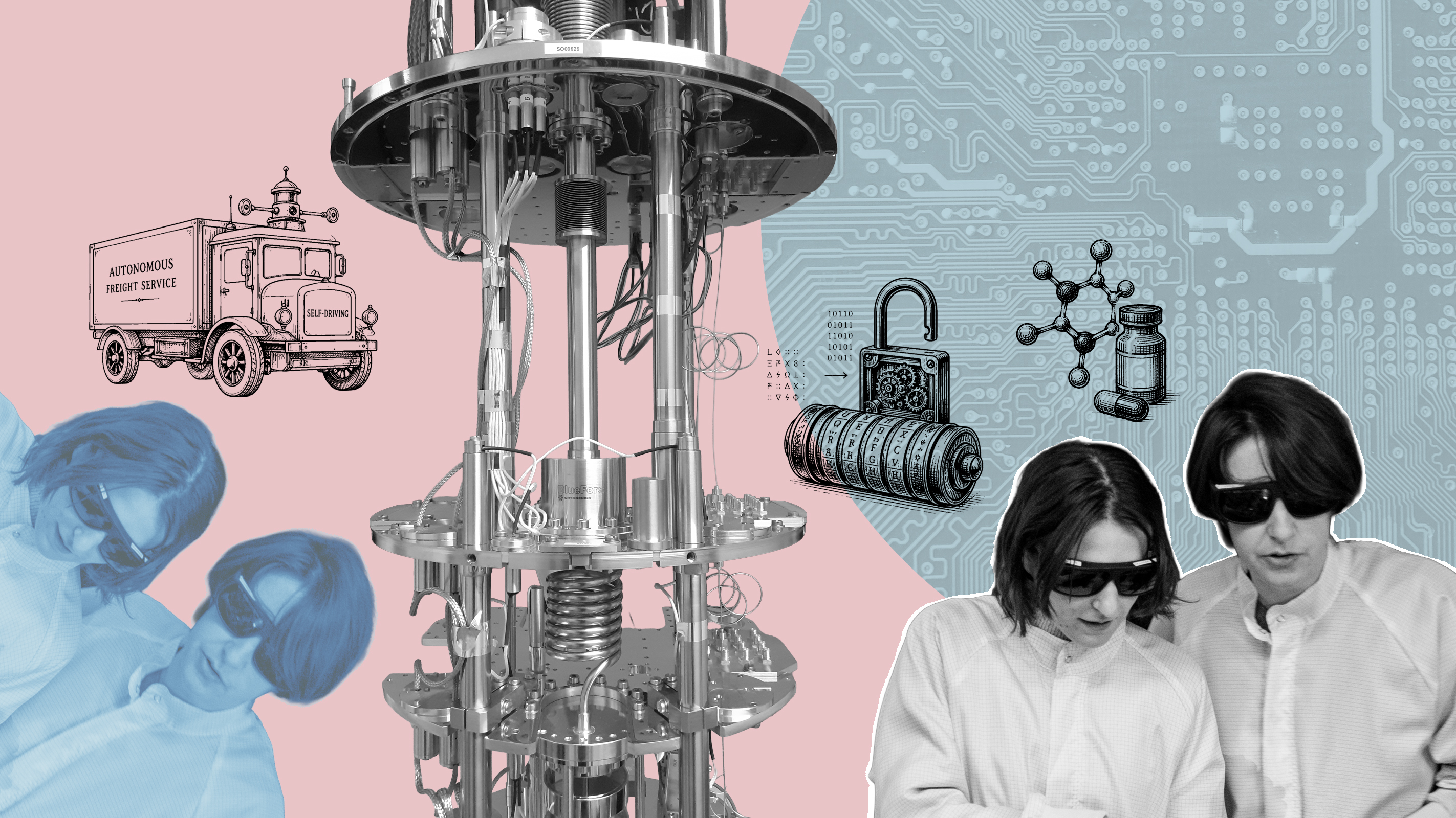
The Profile Area Nanoscience and Semiconductor Technology is part of Sweden’s largest research environment for nanoscience and semiconductor technology and includes world-leading expertise and infrastructures. The area combines scientific theory with laboratory research to find solutions for a sustainable society, the future information society, and the health of the individual.
One goal within the profile area is to achieve a broader understanding of the research field and its applications, and thus remain at the forefront of nanoscience and semiconductor technology.
Our vision is to explore the unique opportunities offered by nanoscience and semiconductor technology and use our cutting-edge research to satisfy fundamental human curiosity, engage in industrial needs, and address societal challenges.
Focus areas
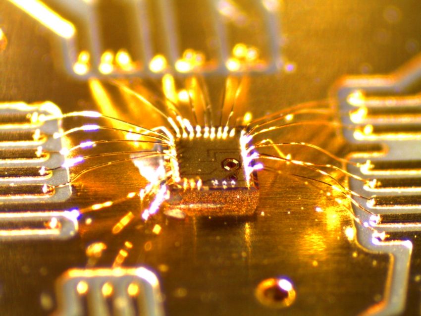
New technology is vital for future communication systems, energy efficiency within both electronics and electrification, and improving renewable energy sources and autonomous systems. The profile area constitutes a critical mass with strong scientific and technical positions in semiconductor material science as well as device and circuit technology connecting both to local and international industry, and into unique infrastructure in Lund.
Research areas:
- Communication and computing technology
- Electrification, energy-saving, and clean energy
- Sensor technology and autonomous systems
Contact: Lars-Erik Wernersson
The area continuously develop and use advanced techniques to characterize and create nanostructures. A challenge is to detect and control changes in the resulting nanostructure that can be caused by atomic-scale changes of formation conditions. To ensure the development of high-quality nanostructures, experiments are combined with theory to enable a fundamental understanding of the material formation process.
Research areas:
- Materials enabling a sustainable society
- Building and understanding devices with atom-level control
- Understanding and improving widespread industrial processes and products
Contact: Anders Mikkelsen
The profile area har internationally leading expertise in the growth, fabrication, and characterization of compound semiconductor nanostructures and rare earth quantum technology, and a strong track record in optical and low-temperature electrical measurements of the quantum properties of nanostructures.
Research areas:
- Quantum technologies based on semiconductor nanostructures and defects in solids
- Pioneering fundamental quantum science
- Novel paradigms for energy harvesting and conversion
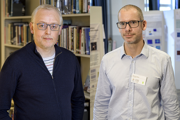
Contact: Martin Leijnse
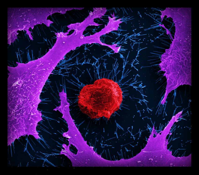
The area develop micro and nanofluidic devices on scales ranging from tens of nanometers to hundreds of micrometers to manipulate, detect and sort biostructures, and strive for a detailed understanding of the interactions between cells and nanostructures with respect to cell behaviour, cell physiology, and cell mechanics. This knowledge makes is possible to develop novel nanoscale devices with applications in biology and medicine.
Research areas:
- Nanobio interactions
- Biological nanoparticles, and single-cell and single-molecule biology and engineering
- Nanoprobes and sensors
- Translation
Contact: Christelle Prinz
NanoLund
NanoLund is the center for research, education and innovation within nanoscience at Lund University. It is a strategic research area funded by the Swedish Government and Sweden’s largest research environment in its field, engaging research groups in the faculties of engineering, science and medicine.
People
Participating departments:
- Biomedical Engineering
- Centre for Mathematical Sciences
- Chemical Engineering
- Chemistry
- Construction Sciences
- Design Sciences
- Electrical and Information Technology
- Energy Sciences
- Mechanical Engineering Sciences
- Physics
Departments from the faculties of Medicine and Science also participate.
Collaboration
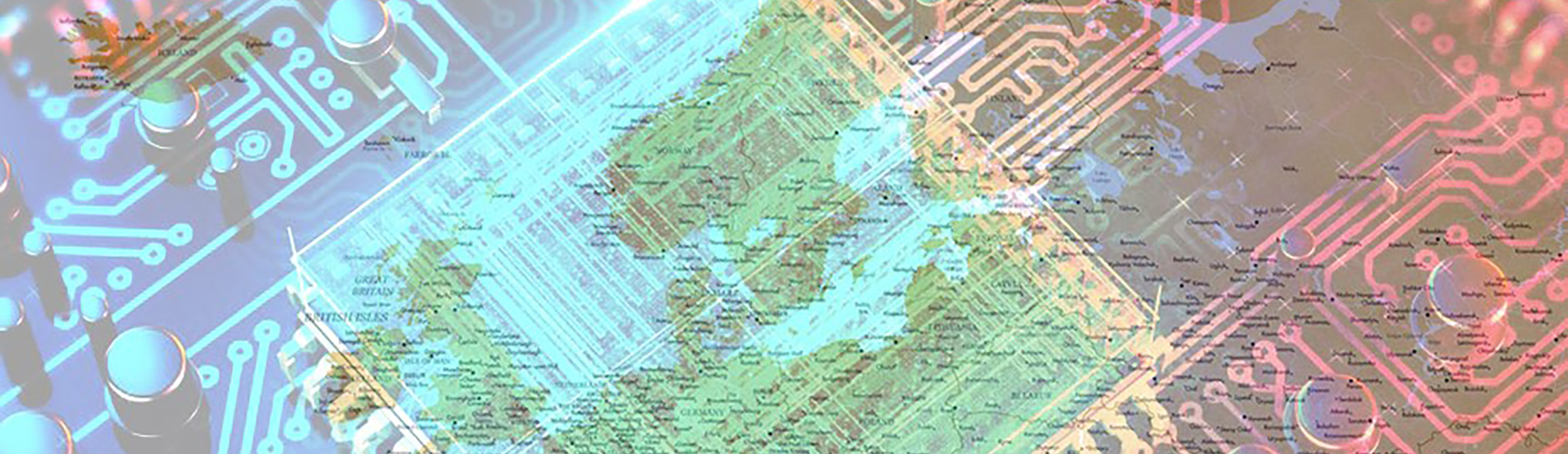
During Sweden’s Presidency of EU in spring 2023, the conference EuroNanoForum was hosted in Lund, with focus on identifying policy options and priorities, plan future actions regarding European activities on the nano field, advanced materials, innovation, sustainability, circular economy as well as materials and energy sovereignty.
The Profile Area Nanoscience and Semiconductor Technology is part of Sweden’s largest research environment for nanoscience and semiconductor technology and includes world-leading expertise and infrastructures. The area combines scientific theory with laboratory research to find solutions for a sustainable society, the future information society, and the health of the individual.
One goal within the profile area is to achieve a broader understanding of the research field and its applications, and thus remain at the forefront of nanoscience and semiconductor technology.
Our vision is to explore the unique opportunities offered by nanoscience and semiconductor technology and use our cutting-edge research to satisfy fundamental human curiosity, engage in industrial needs, and address societal challenges.
Focus areas
New technology is vital for future communication systems, energy efficiency within both electronics and electrification, and improving renewable energy sources and autonomous systems. The profile area constitutes a critical mass with strong scientific and technical positions in semiconductor material science as well as device and circuit technology connecting both to local and international industry, and into unique infrastructure in Lund.
Research areas:
- Communication and computing technology
- Electrification, energy-saving, and clean energy
- Sensor technology and autonomous systems
Contact: Lars-Erik Wernersson
The area continuously develop and use advanced techniques to characterize and create nanostructures. A challenge is to detect and control changes in the resulting nanostructure that can be caused by atomic-scale changes of formation conditions. To ensure the development of high-quality nanostructures, experiments are combined with theory to enable a fundamental understanding of the material formation process.
Research areas:
- Materials enabling a sustainable society
- Building and understanding devices with atom-level control
- Understanding and improving widespread industrial processes and products
Contact: Anders Mikkelsen
The profile area har internationally leading expertise in the growth, fabrication, and characterization of compound semiconductor nanostructures and rare earth quantum technology, and a strong track record in optical and low-temperature electrical measurements of the quantum properties of nanostructures.
Research areas:
- Quantum technologies based on semiconductor nanostructures and defects in solids
- Pioneering fundamental quantum science
- Novel paradigms for energy harvesting and conversion
Contact: Martin Leijnse
The area develop micro and nanofluidic devices on scales ranging from tens of nanometers to hundreds of micrometers to manipulate, detect and sort biostructures, and strive for a detailed understanding of the interactions between cells and nanostructures with respect to cell behaviour, cell physiology, and cell mechanics. This knowledge makes is possible to develop novel nanoscale devices with applications in biology and medicine.
Research areas:
- Nanobio interactions
- Biological nanoparticles, and single-cell and single-molecule biology and engineering
- Nanoprobes and sensors
- Translation
Contact: Christelle Prinz
NanoLund
NanoLund is the center for research, education and innovation within nanoscience at Lund University. It is a strategic research area funded by the Swedish Government and Sweden’s largest research environment in its field, engaging research groups in the faculties of engineering, science and medicine.
Infrastructure
The infrastructures within the Profile Area involves Nano laboratories. The Profile Area is also engaged in MAX IV. Links below will open the respective infrastructure's website.
People
Participating departments:
- Biomedical Engineering
- Centre for Mathematical Sciences
- Chemical Engineering
- Chemistry
- Construction Sciences
- Design Sciences
- Electrical and Information Technology
- Energy Sciences
- Mechanical Engineering Sciences
- Physics
Departments from the faculties of Medicine and Science also participate.
Collaboration
During Sweden’s Presidency of EU in spring 2023, the conference EuroNanoForum was hosted in Lund, with focus on identifying policy options and priorities, plan future actions regarding European activities on the nano field, advanced materials, innovation, sustainability, circular economy as well as materials and energy sovereignty.